This innovative approach offers many benefits, including increased radio frequency (RF) bandwidth, increased information processing capabilities, and universal application across a variety of industries.
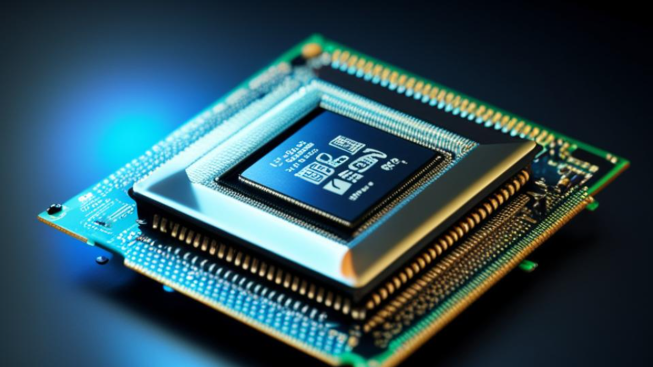
The chip’s ability to integrate electronic and photonic components into a compact silicon package opens new opportunities for the development of advanced radar systems, satellite technologies, wireless networks and 6G and 7G telecommunications.
The chip design uses new silicon photonics technology, which allows the integration of various semiconductor systems less than 5 millimeters in width. This advanced packaging approach, comparable to connecting Lego blocks together, allows electronic and photonic components to be seamlessly integrated, creating a versatile and powerful device.
Source: Ferra
I am a professional journalist and content creator with extensive experience writing for news websites. I currently work as an author at Gadget Onus, where I specialize in covering hot news topics. My written pieces have been published on some of the biggest media outlets around the world, including The Guardian and BBC News.


