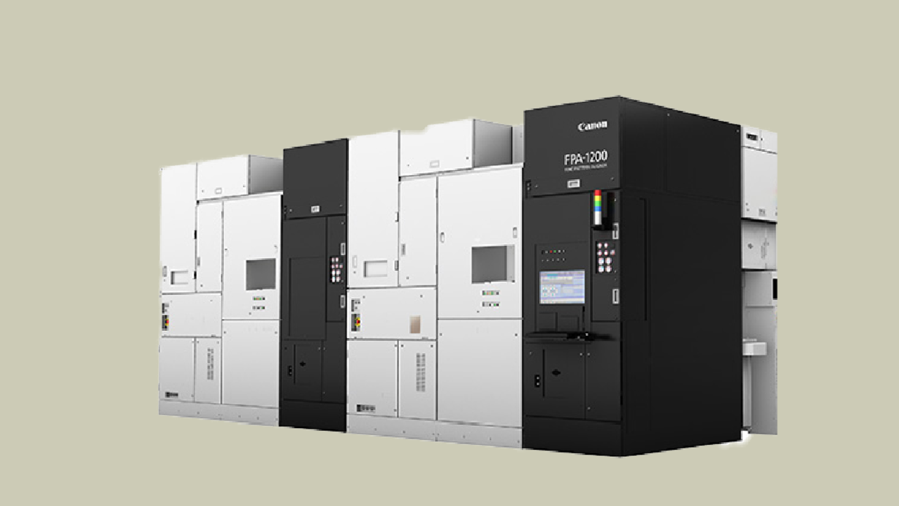
Unlike traditional methods, nanoimprinted lithography eliminates the need for a light source. Instead, it uses the simple principle of transferring a circuit mask to a resistive-covered wafer surface. This technology can create complex 2D and 3D patterns in a single pass and reduce power consumption by approximately one tenth compared to advanced logic exposure methods.
Takeishi said Canon is not looking to compete directly with ASML’s EUV, but instead believes different lithography technologies can co-exist and contribute to overall industry growth. It is reported that companies such as SK Hynix and Kioxia have previously tested Canon machines suitable for high-capacity NAND flash memory, especially with a three-dimensional structure.
Source: Ferra
I am a professional journalist and content creator with extensive experience writing for news websites. I currently work as an author at Gadget Onus, where I specialize in covering hot news topics. My written pieces have been published on some of the biggest media outlets around the world, including The Guardian and BBC News.


