


Smartphones and computers already know how to solve any problem, display realistic graphics in games, and process hundreds of frames per second to create one photo.
The “brains” of all devices are controlled by processors, the development of which helps the industry of our eyes to make leaps in technology.
You’ve probably heard more than once that chips made from natural materials silicon14th element in the periodic table with designation Si.

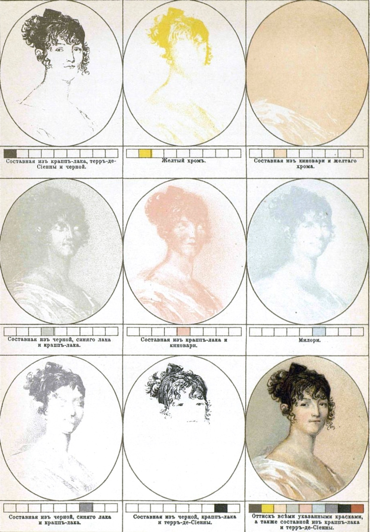
Petersburg, printed by lithography. Below you will understand, here he is
Apple even decided not to bother and keep its processors for Mac simply Apple Silicon, “Silicon from Apple.”
It is the second most abundant element on the planet after oxygen.
But finding it in its pure form is almost impossible. Just highlight.
But we will describe below how a raw mineral is transformed into technological plates with a pattern deep in the molecule. Everything takes three big stages.
Why silicon? It is mined from quartz, which is found in bulk

Silicon uses resources for processors because it is there semiconductor – depending on the batteries nearby, it can be either an insulator or a conductor of electricity. Cost and prefix in the name “semi-”.
In nature silicon (Si) is mined from quartz (SiO2).
There is a lot of quartz all over the planet; the extraction process is inexpensive, and this is another reason for the popularity of silicon.
Sand containing it can be found on any continent on the planet, but the richest are countries with sandy beaches, oceans and rivers.
🤯🌍 More than a quarter (28%) of the Earth’s crust consists of silicon (Si).
Among the leaders in production are the USA, Australia, and Belgium.
The main customers are China, Canada, Japan, Italy.
The entire process of creating chips consists of three large stages: turning the raw material into the purest and most correct structure, preparing a wafer from it and printing the processor.
Stage 1. Sand is boiled, steamed, and then melted
Production of metallurgical silicon
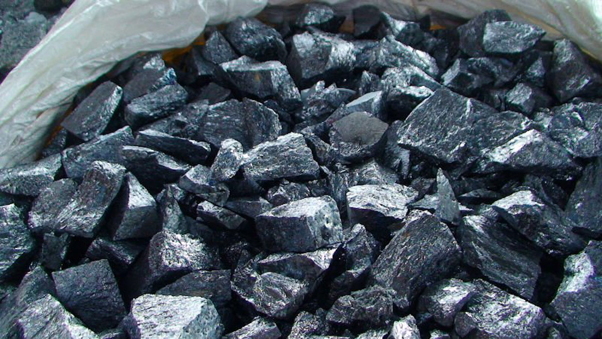
Metallurgical silicon
To make the material suitable for working with it, the extracted sand is tritreated with other substances at high temperatures.
The formula of quartz (SiO2) shows that in it silicon (Si) is associated with oxygen (O).
To separate one from the other and obtain pure silicon, it is ground with coal (C) and poured into an electric arc furnace.
The rods are lowered into the mixture and an electric discharge is given to them. When the heating meter reaches 1900ºC, a reaction occurs resulting in a poisonous gas. oxygen monoxide (CO) and liquid silicon (B) with impurities. Then it freezes and it turns out metallurgical silicon.
Its principle is the production of solar panels, aluminum alloys, paint production, but not for chips.
The purity of the element at this stage is up to 99%, but the remaining percentage must be removed.
Production of polycrystalline silicon

Polycrystalline silicon
To do this, metallurgical flints are mixed at high temperatures with the poisonous gas hydrogen chloride (HCl), resulting in the formation of a gas. trichlorosilane (HCl3Si).
When a gas is cooled to 20°C, it becomes liquid.
Creating pure silicon for chips uses just 1% of Morocco’s metallurgical silicon production.
Next, trichlorosilane is evaporated in another reactor and mixed with hydrogen (O). A reaction occurs (called “chemical vapor deposition”), and the purest silicon is deposited on the rods prepared in the reactor. The released chlorine and hydrogen are converted into gas.
We are almost at the last stage.
Pulling a silicon crystal like this takes about 140 days.
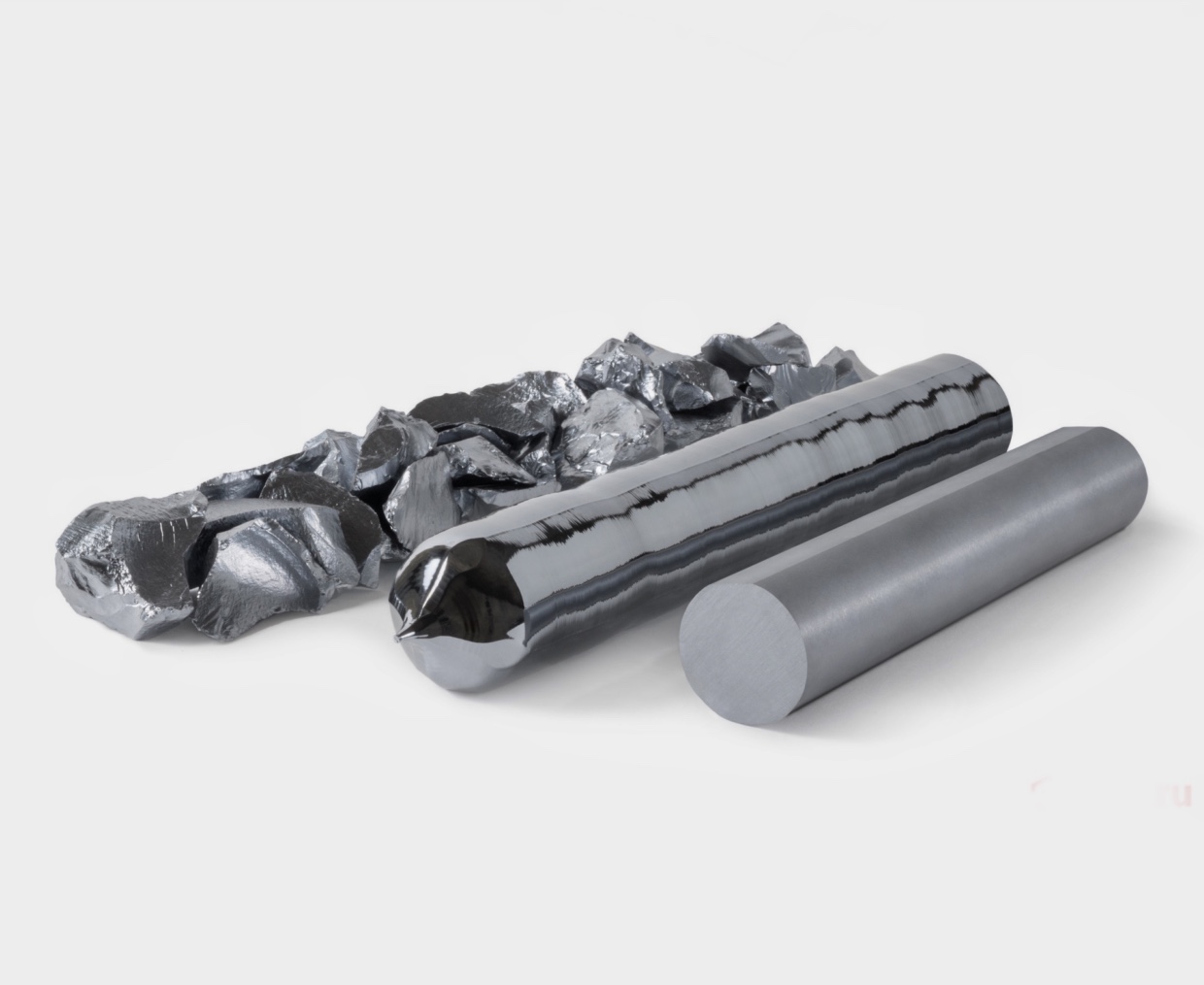
Silicon crystal with a logical structure in the center
The resulting silicon is called polycrystalline. It is suitable for the manufacture of, for example, solar panels. But its molecular structure is chaotic and therefore fragile.
To create pure crystalline silicon, the material is heated and then left to sit. 140 days grow onto the rod, gradually pulling it out of the container. The purity of this silicon is such that only 1 atom in 10 million atoms is not silicon.
It turns out single crystal silicon – the final form of the material that ends up in your smartphone.
Stage 2. Stone pancakes make perfect texts
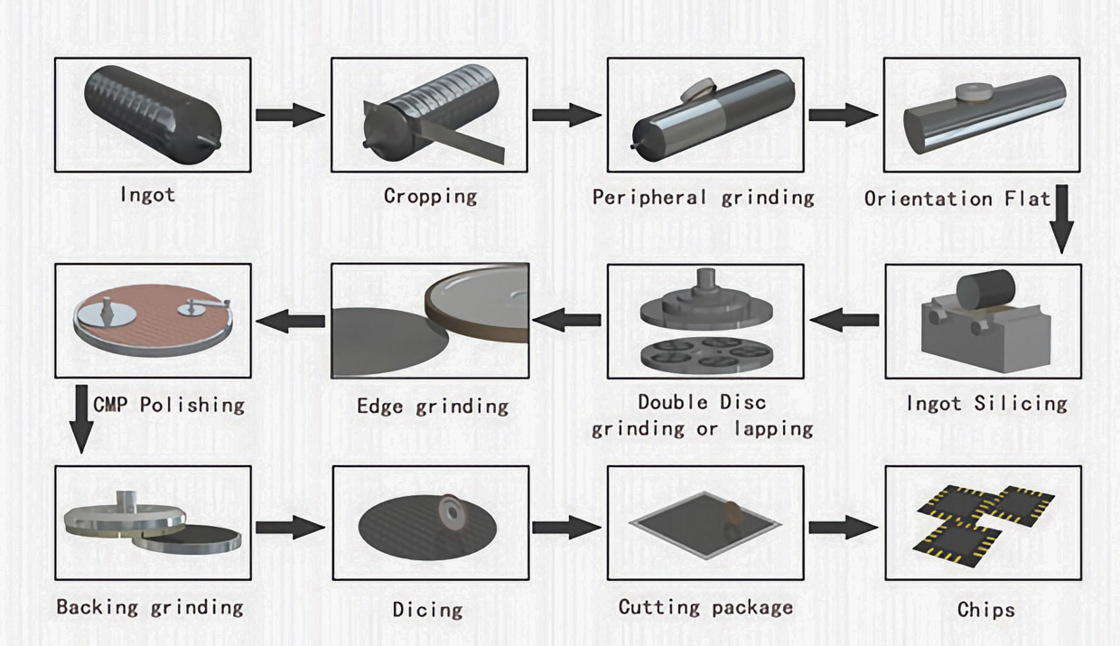
Apart from the last two, these are all the stages of turning a silicon crystal into the basis for chips.
The chips are “printed” on a layer of silicon, which is obtained from this crystal. To make it perfectly smooth, the stone goes through several stages.
Due to the “pulling”, the crystal has shoulders that are cut off with a powerful saw, and due to vibrations during growing, it is uneven, which is solved by grinding the outer layer.
cream The next one is cut into thin pancakes using a diamond wire. The plates are then polished with a diamond machine. Their edges are rounded so that the panels do not crack under heavy loads during printing. They will be heated, oxidized, vaporized and irradiated ten times.

Cutting the crystal into wafers
Grinding silicon wafers
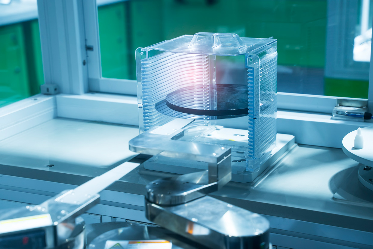
Using a bath and a centrifuge, the polished “wafers” are cleaned of metal contaminants and dust.
They go through a cleaning stage with both liquid and gas compounds to create a perfectly flat surface for the next stages.
The result is pancakes with a diameter of up to 300 millimeters and a thickness of no more than a millimeter.
A few bases. How silicon is reversed in zero and important value
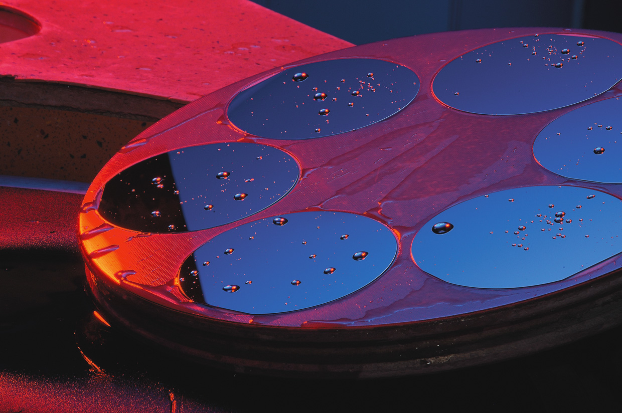
Electronic chips with billions of transistors are printed on sliced silicon wafers.
I will give out premises to reach the last stage.
Transistors play the role of the basic building blocks in any modern chip. The more there are, the better. There can be billions of them in one processor, which, for example, Apple talks about at each of its presentations.
In addition to the number of transistors, their size, design, materials, sensitivity, and connection to each other are important.
The efficiency of the design of all these methods determines the speed of the chip.
This building block operates a simple mechanism. When enough current is supplied, the transistor will drive a charge through itself – this is a “one”. If the current is sufficient, the transistor does not conduct a charge – it outputs “zero”.
Depending on how much energy the transistor requires to “activate”, the same energy efficiency of the chip is used. Sensitivity, in turn, depends on the size of the transistor.
![]()
I made a simple transistor circuit for you. In fact, they have different structures and compositions of materials.
In the picture above you can see that no current flows through the white contact in the center. The transistor is at rest.
Three basic elements are responsible for the operation of the transistor: source (negative charge), base (n-type semiconductor + polycrystalline silicon gate) and collector (positive charge).
Each element has contacts. In modern processors, the role of contacts is played by a nanometer layer of metal.
p-type semiconductor – silicon saturated with boron. In such a material there is room for the last electrons, since there is 1 External fewer electrons than silicon (three versus four).
There are two of them in the picture above: on Istoshik a negative charge is applied to collector positive.
n-type semiconductor – silicon, saturated phosphorus. This material has one extra electron because phosphorus has five different electrons versus four for silicon.
In the picture above he is alone, this is base.
Red highlights “gate” from polycrystalline silicon. Activation occurs through them. If enough energy is applied to this central element, it begins to attract electrons from the large orange n-silicon base to the center.
![]()
![]()
![]()
Real photo of the transistor. Left collector, in the center of the “gate”, to the right of the source
This creates a bridge between two p-conductors, and the current between them becomes looped. The circuit is closed, the state is “one”.
And these operations happen billions per second in your smartphone processor, watch, computer and headphones.
But how does this construction set assemble at the molecular level?
Stage 3. Processors are burned out using stencils

Chips are printed using different technologies; here one of the newest products is with several masks at the same time. One such machine from ASML costs about $200 million.
Since we are talking about dimensions in the nanometer range, with mechanical tools it is clear that all its components cannot be elements.
Processors literally print layer after layer onto silicon using lithographs. Previously, prints were made on the figure and model in this way, but in our case the process is more subtle.
A simple processor lithography scheme is as follows:
1. Put on a layer of building material.
2. There is polymer on it. Gives a stencil on top
3. The polymer hardens in open doors under the influence of ultraviolet radiation.
4. Clean everything that has not hardened (polymer + silicon)
5. Repeat at the new cost once until the required structure.
☝️Paintings are painted using the lithography method in the same way. First one layer of color, then a second and so on. Somewhere they intersect and form a complex material.
Using a centrifuge, a layer of the required material described above is evenly evenly applied to pure silicon. This component has the shape conceived by the engineers – each stage uses a different element.
Next, a layer of polymer photosensitive material is applied to the surface. Then a stencil is formed in each processor at each stage of its development.
Accelerated lithography scheme, if the plate were not cleaned at each stage of excess after irradiation. Source here
The laser irradiates the plate. Wherever the light hit, it became solid. Wherever it is, the place is completely cleaned to the required layer of engineers: heated, sprayed with chemicals, doused with gas.
The polymer is removed, the element underneath remains in its usual shape, the rest is cut out.
Then a new layer with the desired element is applied, covering it again with polymer. Fired with a stencil again, this time in a new form. Cleaning up what hasn’t hardened again.
Factory TCMC, the main manufacturer of Apple processors
One of the chips for printing
And so on, maybe a hundred layers, until the intended engineering design of a processor consisting of billions of transistors is printed on silicon.
During these procedures, the silicon may be heated, bathed, and burned ten times to ensure a successful print.
Once all lithography steps are completed, the wafers are inspected through a microscope, cut, and layered on top of each other onto a single chip.
That’s why technology is “high”
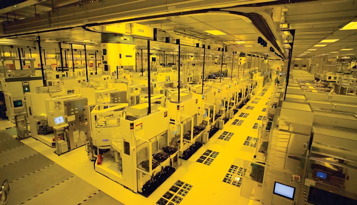
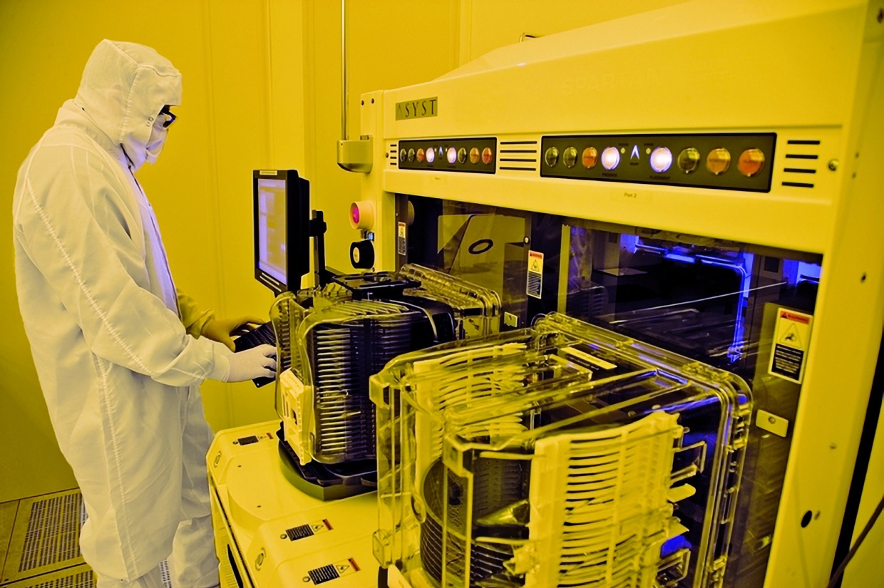
Lithography laboratories have perfect sterility. Employees are prohibited from wearing makeup, wearing rings, smoking or wearing perfume.
The rooms purify the air non-stop so that not the slightest particles get onto the silicon wafers.
Engineering quality control is carried out using a microscope.
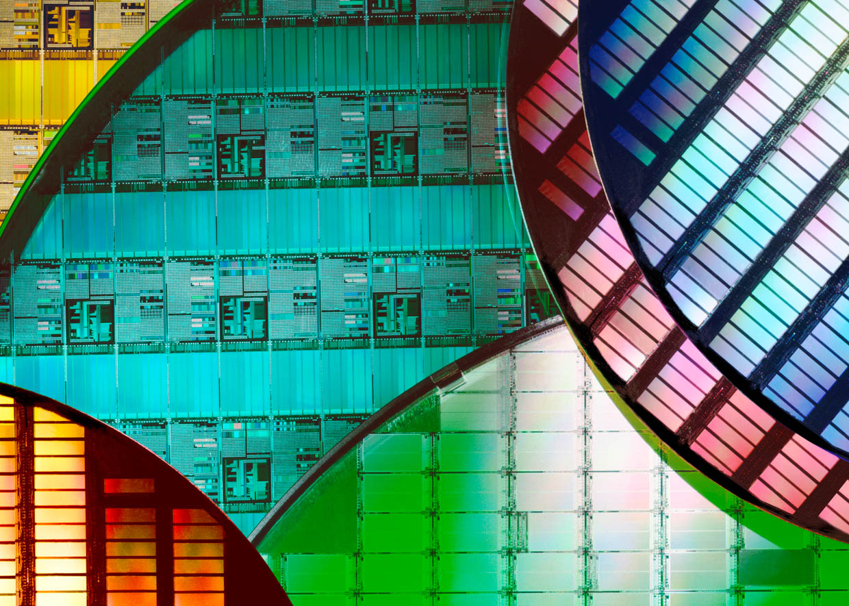
And as a result, after printing, the waffles get a golden-rainbow hue, because On the surface of the stone, a perfect pattern of transistors is obtained, which include various types of metal deposits and silicon composites several molecules thick..
There is a main difficulty in the progress of transistors: in order to consume less current, they must become thinner, for this they need to be made smaller. That’s why engineers are developing new structures to smarterly limit the conductors within the frame. That’s why, for example, Apple says that the graphics processor in the A17 Pro from the iPhone 15 Pro has been completely redesigned.

And for the same reason, Apple has achieved high energy efficiency with Arm technology. Engineers find it easier to work with transistors that are designed with this design in mind.
And for the same reason, for example, the A16 from the iPhone 15 and iPhone 14 Pro is more powerful than the Qualcomm Snapdragon 8 Gen 2, although both cases have 16 billion transistors. Apple, of course, used a more efficient arrangement of each building block when referring to each other, and it tailored it to its software.
Because the moment the stone turns into smart hardware, developers begin to sharpen it for their operating systems.
◇ Stove for gamers. I played Genshin Impact on an iPhone 15 Pro Max and got burned
◇ I figured out in a week how the hype ChatGPT works. No magic
◇ iPhone 15 Pro and iPhone 14 Pro alignment camera. Is there a difference, let’s look together
Source: Iphones RU
I am a professional journalist and content creator with extensive experience writing for news websites. I currently work as an author at Gadget Onus, where I specialize in covering hot news topics. My written pieces have been published on some of the biggest media outlets around the world, including The Guardian and BBC News.

: Everything we know a week after its release")


